As chip manufacturers edge ever closer to the limits of what can be achieved with silicon, researchers have been exploring ways of boosting performance and power efficiency by stacking other components. One such group from MIT has pushed the boundaries of what seemed impossible just a few years ago, though, by developing a technique to attach GaN transistors onto a silicon chip, which could lead to even better wireless devices.
If you’ve bought a decent charger for a laptop, phone, or other mobile device recently, there’s a good chance it’s a GaN-based one. Gallium nitride (GaN) is a semiconducting material like doped silicon, but when it comes to dealing with high temperatures, voltages, and current transmission, GaN has the latter well and truly beat.
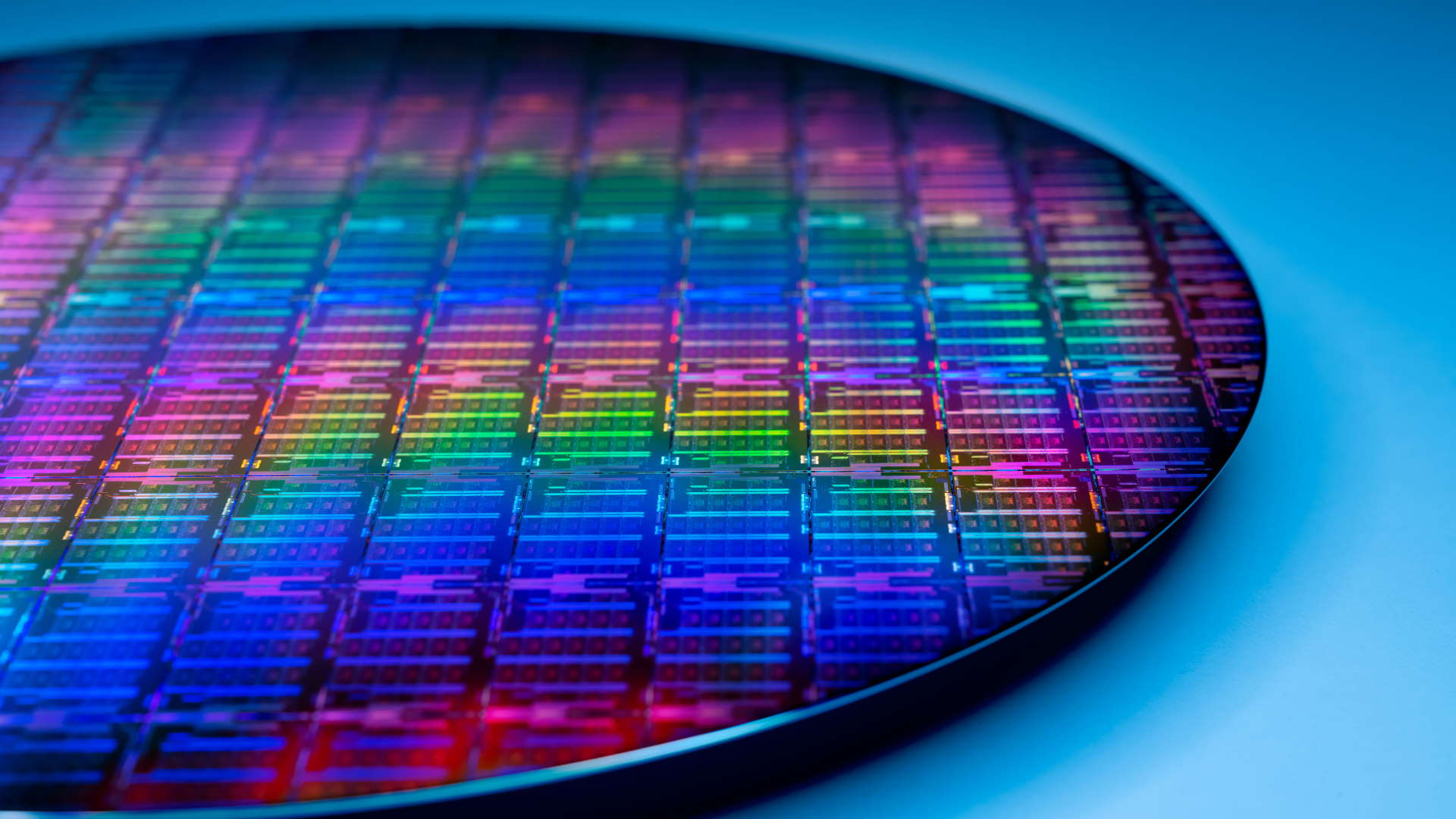
Hence why it’s the top pick for any device that needs to operate at super high frequencies or handle a lot of power. Unfortunately, a wafer of chips made entirely from GaN is considerably more expensive than the common-or-garden wafers that produce the millions of chips used in PCs, consoles, TVs, phones, and all the rest.
This is precisely why a team of researchers based at the Massachusetts Institute of Technology (MIT) and other centers have developed a method that allows for GaN transistors to be stacked on top of a normal silicon chip, so that the design gets all the nice GaN benefits in the right place but without incurring the high cost of stacking an entire wafer.
“We wanted to combine the functionality of GaN with the power of digital chips made of silicon, but without having to compromise on either cost of bandwidth. We achieved that by adding super-tiny discrete gallium nitride transistors right on top of the silicon chip,” said Pradyot Yadav, a graduate of MIT and the lead author of the paper on this method.
To clarify something important, it’s worth noting that Yadav isn’t talking about transistors the size of those in your AMD or Intel CPU. Strictly speaking, the method is creating what electronic engineers call a dielet (a bit like a chiplet), and in this case, the dielets are 0.24 x 0.41 mm in size.
These are laser-cut from a GaN wafer, which has copper interconnects already attached, making it much easier to then attach the dielet to a traditional silicon die. MIT notes that most bonding techniques like this require the use of gold, which is not only more expensive than copper but also requires the whole setup to be heated to a level that can potentially damage the incoming dielet and host die.
Once the researchers had perfected the manufacturing process, they created a power amplifier from it, using a silicon chip made via Intel’s 22 nm process node. The end result was a tiny circuit that can boost an electromagnetic signal more than a traditional silicon design. Unfortunately, the paper is behind an academic paywall, so it’s not clear just how much better the copper-bonded GaN-dielet amplifier is than a normal one.
But even if it’s only a little better, you can be sure that the likes of Intel and Qualcomm will be looking at the research with interest. That’s because it’s becoming increasingly harder, and thus more expensive, to have silicon chips running faster and handling more power. 3D stacking is not only the future of processors, but smaller components too, and the WiFi and Bluetooth transmitters in phones, consoles, and PCs of the future will almost certainly go down this route.
For me, if I can just have a set of Bluetooth headphones that don’t disconnect from my PC because I’ve dared to move my head by all of three inches, then I’ll gladly pay a bit more for a superstacked GaN transmitter.