- Sandisk enlists top computing minds to shape flash-based memory alternative for AI
- HBF memory backed by RISC and GPU leaders promises high bandwidth and massive capacity
- Patterson and Koduri join Sandisk to guide flash memory expansion beyond HBM limits
Sandisk has appointed two leading figures in computing to help shape the direction of its high-capacity memory tech for AI workloads.
Professor David Patterson and Raja Koduri have joined Sandisk’s new Technical Advisory Board to provide strategic and technical input on High Bandwidth Flash (HBF), a flash-based alternative to High Bandwidth Memory (HBM).
Patterson is credited for co-developing Reduced Instruction Set Computing (RISC) and Redundant Array of Inexpensive Disks (RAID), and will lead the advisory board. Koduri is known for his leadership in graphics architecture, having overseen GPU designs at AMD and Intel.
Decades of experience
Together, they bring decades of experience across computing, memory systems, and large-scale architecture.
“We’re honored to have two distinguished computer architecture experts join our Technical Advisory Board,” said Alper Ilkbahar, Executive Vice President and Chief Technology Officer at Sandisk.
“Their collective experience and strategic counsel will be instrumental in shaping HBF as the future memory standard for the AI industry, and affirming we not only meet but exceed the expectations of our customers and partners.”
Patterson said, “HBF shows the promise of playing an important role in datacenter AI by delivering unprecedented memory capacity at high bandwidth, enabling inference workloads to scale far beyond today’s constraints. It could drive down costs of new AI applications that are currently unaffordable.”
Koduri added, “HBF is set to revolutionize edge AI by equipping devices with memory capacity and bandwidth capabilities that will support sophisticated models running locally in real time. This advancement will unlock a new era of intelligent edge applications, fundamentally changing how and where AI inference is performed.”
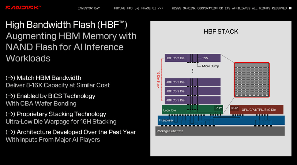
HBF is designed to match the bandwidth of HBM while offering up to 8 times the capacity at a similar cost.
Built with BiCS flash, CBA wafer bonding, and proprietary stacking that allows 16 dies per package, HBF offers a new way to expand GPU memory without relying entirely on expensive DRAM.
While not a direct replacement for HBM, HBF shares the same electrical interface and only requires minimal protocol changes.
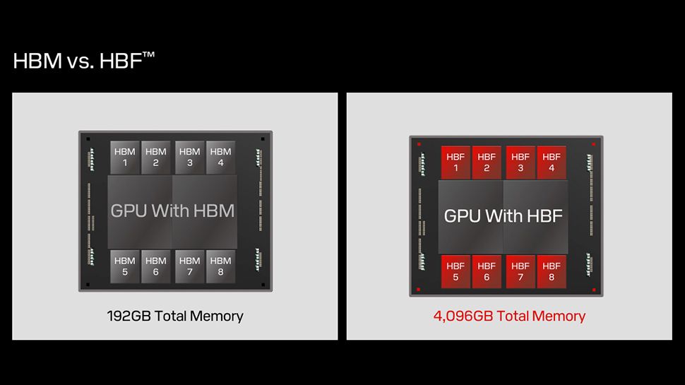
Sandisk previously demonstrated how an AI GPU using only HBM might support 192GB of memory, but by combining it with HBF, that figure could reach 3TB.
In a configuration using only HBF, memory capacity could scale up to 4TB.
The technology was first revealed at Sandisk’s Future FWD 2025 investor event back in February 2025, alongside its roadmap for future HBF generations.
These updates show increases in capacity and bandwidth over time, with some tradeoffs in energy efficiency.
By forming an advisory board and seeking open standard development, Sandisk is trying to avoid locking the market into proprietary solutions.
This may help it gain traction against rivals like Samsung and SK Hynix which are both heavily invested in the HBM space.